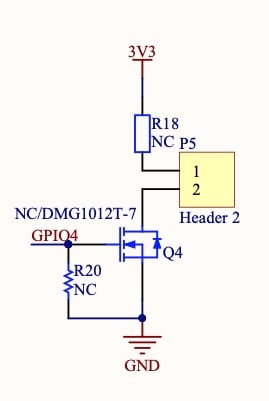
This is from a module I'm using and I don't understand this part of it. https://files.waveshare.com/upload/3/3c/RP2040-Touch-LCD-1.28.pdf
Electrical and computer engineering (ECE) community, for professionals and learners. Discuss ECE related topics here, for instance digital design, signal processing, circuit analysis, electromagnetics, microelectronics, power electronics, RF electronics, etc.
This is from a module I'm using and I don't understand this part of it. https://files.waveshare.com/upload/3/3c/RP2040-Touch-LCD-1.28.pdf
It looks like an n channel mosfet connecting the negative pin of the header to ground, with a resistor to keep the gate low (and consequentially keeping the mosfet on) until pulled high by gpio 4
That's a MOSFET, I always get confused if its n-mos or p-mos. Based on context, it looks like an nmos to me, enhancement mode.
MOSFETs are a voltage-controlled resistor. When GPIO4 is below the "threshold voltage", the other two pins have a resistance of roughly 1-Gigaohm or so (basically disconnected). When GPIO4 is above the "threshold voltage", things get very complex so lets... ignore the threshold region.
But once voltage gets "high enough", then the resistance between 2-and-ground will drop to ~5 ohms to 0.05ohms, depending on the model of MOSFET. (The more expensive the MOSFET, the lower the resistance gets).
The diode is called the "body diode", its innate to MOSFET construction. Its not a real diode you place, but instead just how MOSFETs work (MOSFETs are built on top of P-N doped junctions, so the Drain-pin and Source-pin have an effective diode across them)
In some cases, the Gate (aka: GPIO4 in this picture) has a voltage-protection circuit on it. That pin is famously sensitive to static electricity. If you ever put static-electricity on there (ex: walk across a carpet while holding onto that pin), the MOSFET can be damaged and could very well not function anymore. But many MOSFETs do not have any voltage-protection at all, so be careful.
The three pins on the MOSFET by the way, are named "gate", "drain" and "source". You may have heard of "Vss" and "Vdd", this means "Voltage at Source" and "Voltage at Drain", because most chips are MOSFET based. BJTs have similar pin names: "base", "emitter", and "collector", and you may have seen Vcc (aka: Voltage at the collector) before in various notes when those devices are made out of BJTs internally.